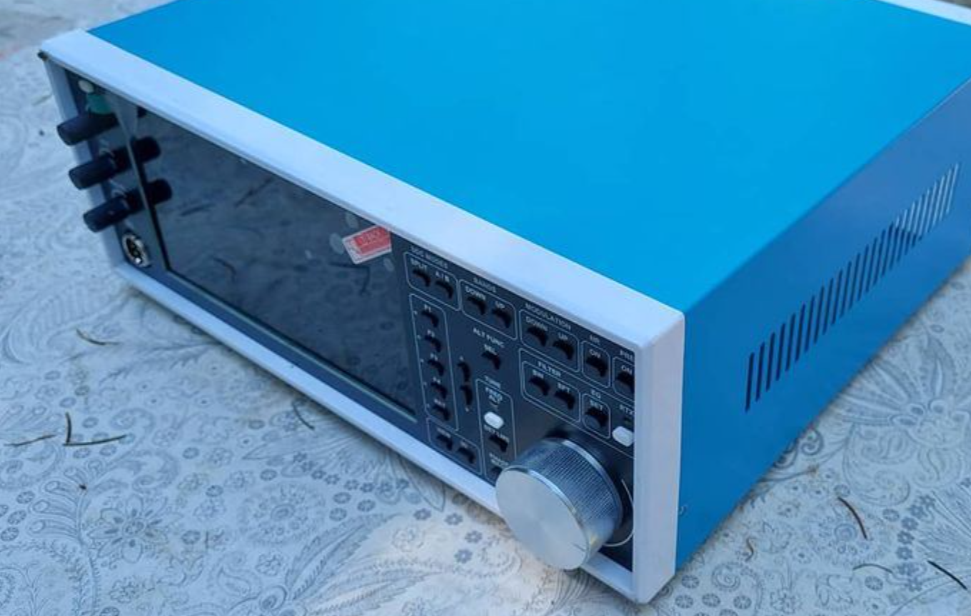
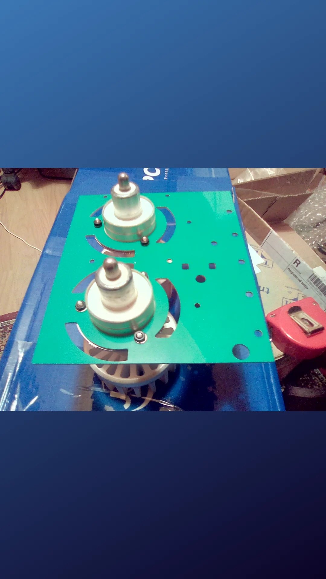
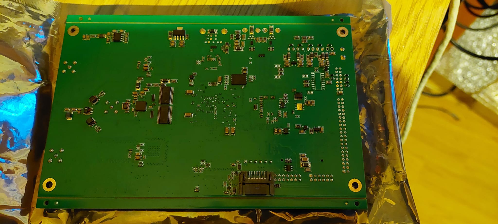
STM32 controller. Diff RF decoupled from 12VDC power supply. 7 ADC multiplexed inputs for DC U/I measurements as RFDSP voltage and current, PA voltage and current, VSWR voltages on VSWR bridge). Hole for one optical encoder. Holes for two mechanical rotary encoders - MULTI and ATT, one analog potentiometer for volume control on ADC. All inputs are RF and ESD protected. USART for communication with baseboard. (this architecture was tested in my H7R SDR)
- the RF inputs are not BW limited - can work in subsampling mode up to 400 MHz+ (depends on RF input transformers BW)
- 1x 14b D/A - 0...60 MHz RF (fNyq) output
- LVDS connection
- the RF output is not BW limited
- 2x USB2 on ARM
- 1x USB3 on FPGA
- 7 series FPGA, BGA 484, XC7A35T (or 50T, or maybe 75T or 100T also)
- Allwinner T113-S3 dual core 1.2 GHz ARM
- CPU clock from FPGA - LVDS connection
- 7'' TFT, 16b
- up to 50 MHz+ CLK (tested)
- 12 Layer PCB, controlled impedance
- I2S, SPI, IO connections between FPGA and ARM
- TLV320 audio codec
- Stereo HPHONE and LINE output
- 2W audio PA
- ESD and RF protected audio line outputs (into codec)
- ESD and RF protected Optical Encoder input (for tuning)
- ESD protected and Opto-coupled input for CW key
- ESD and overcurrent protected I/Os, USART, SPI, I2C on connectors
- SYNC signal output for DCDC power supply module - LVDS connection on SATA connector
- USART debug port
- Differentially decoupled and Synchronized power supply on separate PCB
- Dedicated for HF SDR or for measurement tools
- Very high SNR and SFDR performance
- SDR FW development in progress
- @NOTE The Fs of baseband i/q signal is 96 kHz - 2x 96 kHz slot used for two DDC channel
- implemented on FPGA side:
- two independent DDC running in parallel at 122.88 MHz
- the 2x 16b signals from two ADC running in parallel and synced to one output clock of ADCs
- SUMming baseband channels with phase shift and magnitude scale (cordic level)
- I2S communication protocol
- SPI communication protocol
- 24 MHz clock output from PLL to ARM - LVDS output
- implemented on ARM side:
- I2S communication protocol to FPGA - (2x 96 kHz slot used for two DDC channel)
- SPI communication protocol to FPGA
- two CIC freq. compensation filter - two Waterfall and Spectrum plot (A/B) at a time - two Baseband Channel processed at a time - NR - high performance noise reduction
- user graphics
- See some tests at the end of this page (uploads in progress)