Hova süllyedt a rádióamatőrködés is, „egészen elképesztő”. Röviden csak ez jut eszembe: „nem kell hozzá művészet, csak hangerő”, vagyis kevés kivételtől eltekintve a tudás már kihalt, szakmaiatlanná vált az egész.
2026. augusztus 9., vasárnap
Idiotizmus, szakmaitlanság, kóklerség
"Egészen elképesztő", hogy néhány HR-es idiótán, kókleren múlik sok mérnök szakmai fejlődése és megélhetése. Eppen most mondtad el az inter(júh)n , hogy beágyazott területen SoC bare-metal programozással is foglalkozol, erre megkérdezi, hogy: "és mikrovezérlőkkel is dolgozott?"
A CV-t nem ildomos elolvasni két kávézás között. Az egy dolog, hogy a szakmai CV-ből a HR-esek nagyrésze semmit nem ért, de el sem olvassa.
Fáj a nájn, azt kész van.
Hova süllyedt a rádióamatőrködés is, „egészen elképesztő”. Röviden csak ez jut eszembe: „nem kell hozzá művészet, csak hangerő”, vagyis kevés kivételtől eltekintve a tudás már kihalt, szakmaiatlanná vált az egész.
Hova süllyedt a rádióamatőrködés is, „egészen elképesztő”. Röviden csak ez jut eszembe: „nem kell hozzá művészet, csak hangerő”, vagyis kevés kivételtől eltekintve a tudás már kihalt, szakmaiatlanná vált az egész.

XtremeDx H7113R Direct Conversion Transceiver
Key Architecture & Hardware Specs:
Receiver Architecture: Two coherent RF and DDC channels utilizing a hardware-level phasing-add matrix implemented directly inside the FPGA.
Processing: Dual-core ARM Cortex-A7 (1.2 GHz) dedicated to GUI handling and high-level DSP, paired with a custom FPGA fabric.
RF Conversion: 2x 16-bit LTC2208 ADC (122.88 MSPS) and 14-bit TxDAC utilizing full LVDS interfaces.
FPGA-Based Phasing-ADD Mode: A fully hardware-implemented, real-time, running inside the FPGA fabric. It processes the two coherent RX channels, allowing completely independent phase rotation and magnitude scaling per channel.
Interference Mitigation: CNLMS-based I/Q adaptive noise canceling (tested and validated using the same signal on RF inputs).
RF Routing: Two completely independent RX RF routing blocks, each integrating a switchable 20 dB preamplifier, 0.5 dB step attenuator, HPF, and direct ADC access via rear SMA connectors for subsampling/custom front-ends.
Power Amplifier: Delivers 120–140W PEP with 36–38 dB PEP IMD3 linearity across HF + 50 MHz bands.
Audio DSP: Separate 8-band EQ for both Rx and Tx AF signals.
Connectivity: High-bandwidth USB 3.0 (FT601) interface for direct FPGA-to-PC streaming (32-bit Sync FIFO implemented in VHDL) + USB 2.0 for ARM-to-PC communication. AF LINE output, CW-Key input.
Display: 7" TFT panel running a custom UI with a 70 fps refresh rate. It features 2D/3D spectrum views and a dedicated Polar Plot for the Phasing-ADD and ANC modes, visualizing the real-time magnitude and phase rotation per channel.
RF Routing and Linearity Performance: By routing the LTC2208 RF ADC without a preamplifier through the RF router, the system yields its maximum dynamic range and IIP3. Additionally, the 20 dB preamplifier maintains high IIP3 and OIP3 performance. With the internal PGA set to 0, the LTC2208 achieves a theoretical IIP3 of +48 dBm in this specific design.
Receiver Sensitivity (MDS Performance):
CW (100 Hz filter, NR ON): Highly discernible down to -136 dBm (Estimated nominal MDS: -133 to -136 dBm)
SSB (2.7 kHz filter, NR ON): Distinctly audible down to -126 dBm (Estimated nominal MDS: -123 to -125 dBm)
Hardware related details:
.jpg)
Red based Visual Theme - 3D spectrum plot

Blue based Visual Theme - 3D spectrum plot

\Red based Visual Theme - 2D spectrum plot - two Rx Channel View

Red based Visual Theme - 2D spectrum plot - one Rx Channel View

Red based Visual Theme - 3D spectrum plot - one Rx Channel View - Polar plot for Phasing ADD mode - magnitude scale and phase rotating per Rx Channel

Green based Visual Theme - 3D spectrum plot - one Rx Channel View

Green based Visual Theme - 3D spectrum plot - one Rx Channel View - polar plot for ANC (automatic noise cancelling) mode with CNLMS - magnitude scaling and phase rotating possibilities per Rx Channel

Green based Visual Theme - 3D spectrum plot - two Rx Channel View - Main Menu View

Green based Visual Theme - 3D spectrum plot - two Rx Channel View

Tx 8 band EQ
Videos
ANC test using the same signal on RF inputs
2025. szeptember 19., péntek
XtremeDx K160-1 RF Sampler Board
XtremeDx K160-1 RF Sampler Board - Dedicated for HF beamforming
- PCB - 16L, controlled impedance
- FPGA - Kintex 7 - K160 / K325 / K410
- A/D - 4x 130 / 160 MSPS, 16b - LTC2208 / LTC2209 - LVDS connection
- D/A 1x 2 channel 500 MSPS, 14b - LVDS connection
- High speed connections - PCIe 3 x4, SFP, 2x USB3 (connected to MGT, and via FTDI FT601), 2x SATA, MIPI DPHY (output),
- I/O CON { I2S, SPI (LVDS connections), GPIOs }, 2x PLL - LVDS out for processor board sync
- System Clock - used for A/D and D/A and can be used for onboard synthesizer reference clock
- Clock Synthesizer - used for D/A and for PCIe/SFP/(MGT) reference clock
- External System Clock input - U.FL connector - connected to Clock Distributor - for multiple board synchronization
- Sync'd PWR supply on separate board (not showed)

PCB Bottom side

PCB TOP side

PCB TOP side

One HS signal layer

2025. április 22., kedd
SOM module - 4-core ARM Cortex A53
- 4x 1.5 GHz ARM Cortex A53 core
- 2 - 4 GB LPDDR4
- eMMC, NOR FLASH
- High Speed Hirose Connectors
- MCSI, NCSI, HDMI, LVDS display, 2x I2S, I2Cs, SPI ,...
- Sync power supply and high DCDC noise reduction (for SDR applications)
- 4x USB2
PCB development in progress.

2024. december 9., hétfő
XtremeDx SDR - USB3/FT601 interface implementation
Implementation of USB3.0 Super-Speed 32 bits Sync FIFO interface

- 1V8 I/O voltage, 67 MHz bus CLK
- written interface code in VHDL
- interface simulation using a few data bytes
- the loopback test is working with 1kB data
- PC app - FT601 loopback demo app

Zoomed
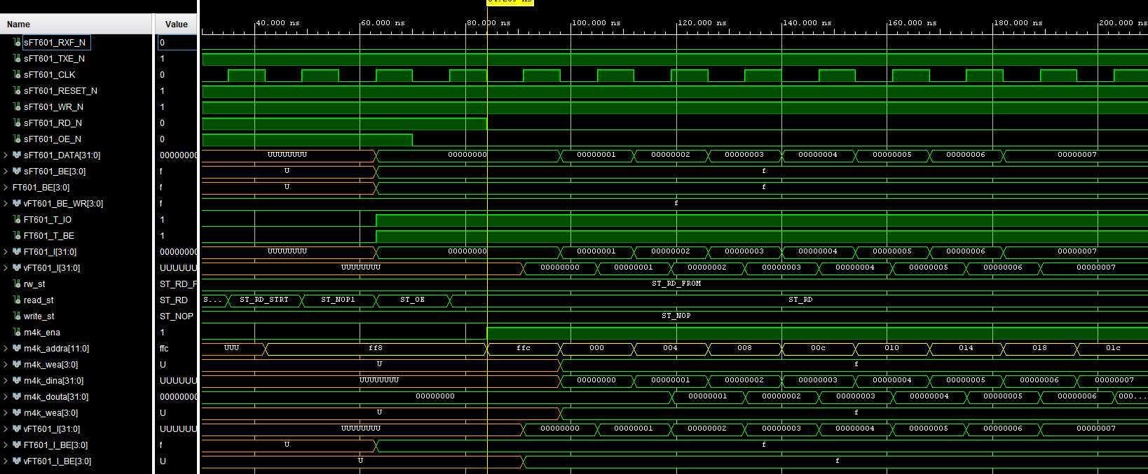
FT601 interface VHDL code - part 1 - the concept

2024. október 23., szerda


2024. szeptember 6., péntek
HF Tx router
I2C controlled HF Tx router
- 50 MHz Nyq filter
- Tx preamplifier
- preamplifier BIAS on/off by i2c
- direct signal routing on/off by i2c
- fixed value ATT on preamplifier in/out
- DC blocking and ESD protection at input

Feliratkozás:
Bejegyzések (Atom)