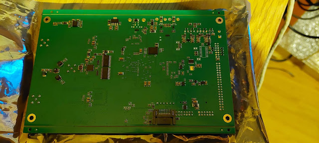
- 2x 16b A/D (LTC2208) - 0...60 MHz RF (fNyq) input
- LVDS connection
- the RF inputs are not BW limited - can work in subsampling mode up to 400 MHz+ (depends on RF input transformers BW)
- 1x 14b D/A - 0...60 MHz RF (fNyq) output
- LVDS connection
- the RF output is not BW limited
- 2x USB2 on ARM
- 1x USB3 on FPGA
- 7 series FPGA, BGA 484, XC7A35T (or 50T, or maybe 75T or 100T also)
- Allwinner T113-S3 dual core 1.2 GHz ARM
- CPU clock from FPGA - LVDS connection
- 7'' TFT, 16b
- up to 50 MHz+ CLK (tested)
- 12 Layer PCB, controlled impedance
- I2S, SPI, IO connections between FPGA and ARM
- TLV320 audio codec
- Stereo HPHONE and LINE output
- 2W audio PA
- ESD and RF protected audio line outputs (into codec)
- ESD and RF protected Optical Encoder input (for tuning)
- ESD protected and Opto-coupled input for CW key
- ESD and overcurrent protected I/Os, USART, SPI, I2C on connectors
- SYNC signal output for DCDC power supply module - LVDS connection on SATA connector
- USART debug port
- Differentially decoupled and Synchronized power supply on separate PCB
- Dedicated for HF SDR or for measurement tools
- Very high SNR and SFDR performance
- SDR FW development in progress
- @NOTE The Fs of baseband i/q signal is 96 kHz - 2x 96 kHz slot used for two DDC channel
- implemented on FPGA side:
- two independent DDC running in parallel at 122.88 MHz
- two Waterfall and Spectrum plot (A/B) at a time
- two Baseband Channel processed at a time
- NR - high performance noise reduction
- See some tests at the end of this page (uploads in progress)
2023-05-02 - PCB development DONE
2x USB2, USB3 connections and FPGA, CPU capacitors
First tests - under development


Nincsenek megjegyzések:
Megjegyzés küldése